PCB Defect Detection
This project was designed and developed as a practical assignment (TP) for the Artificial Intelligence course, specifically in the Computer Vision module. It applies state-of-the-art convolutional object detection models (YOLO11) to a concrete industrial engineering problem.
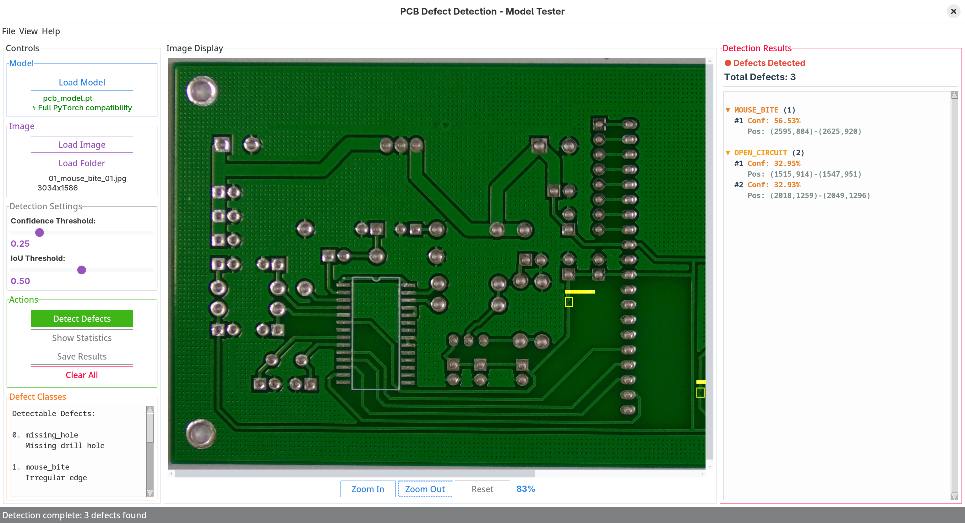
Why Automate PCB Inspection?
In the electronics manufacturing industry, visual inspection of raw printed circuit boards (PCBs) is traditionally manual or reliant on expensive optical systems. Human inspection is slow, fatigue-prone, and error-prone. A single undetected defect (such as a short circuit, broken trace, or missing hole) can cause component destruction during assembly or total hardware failure.
The Computer Vision Solution
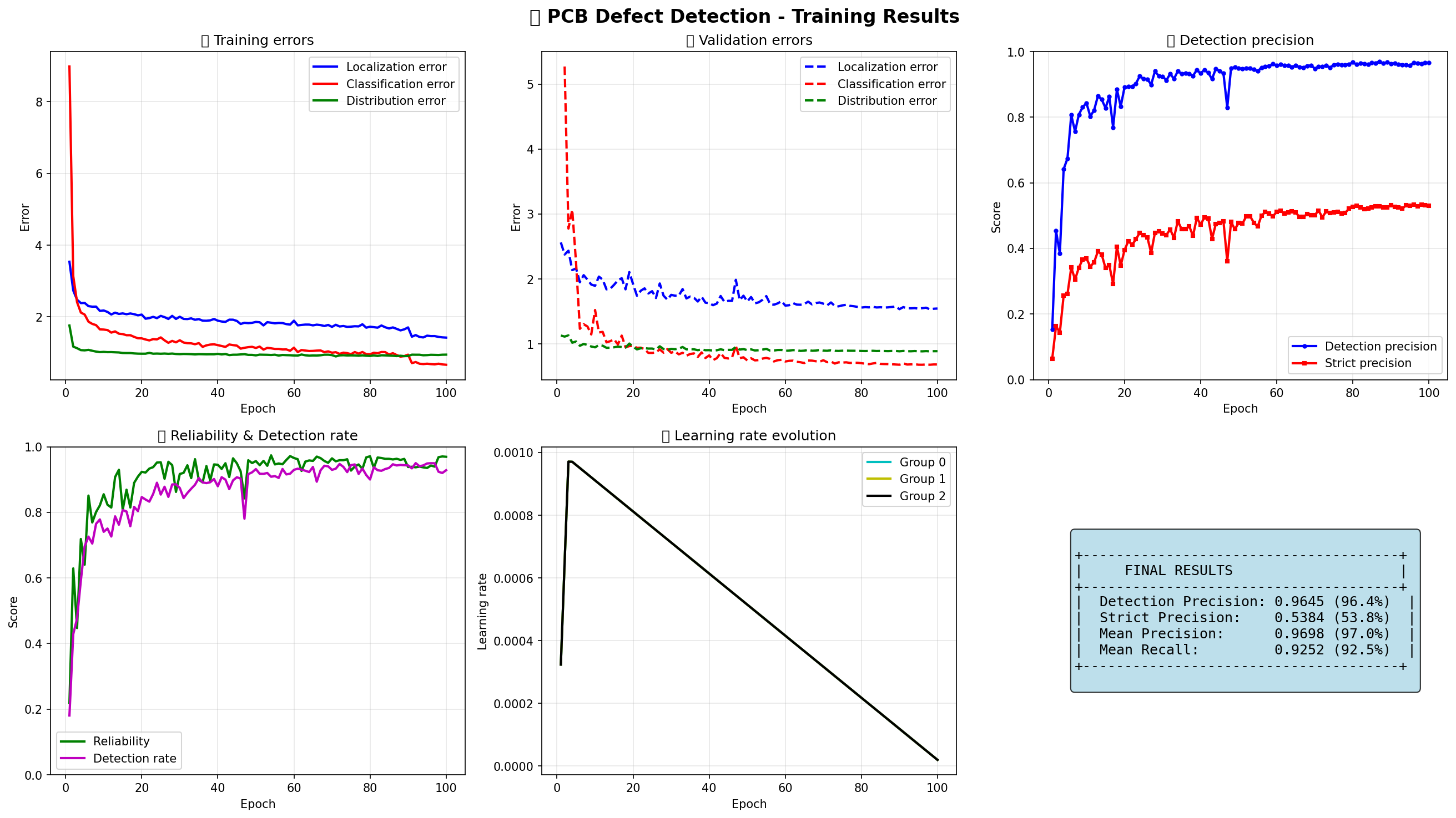
I chose this topic to bridge electrical/electronic engineering with artificial intelligence. AI-driven defect detection (YOLO11) provides an automated, ultra-fast (real-time GPU inference), and affordable solution reaching 97.4% precision, ensuring circuit reliability before component assembly.
YOLO11 Model Performance
Detected PCB Defect Classes
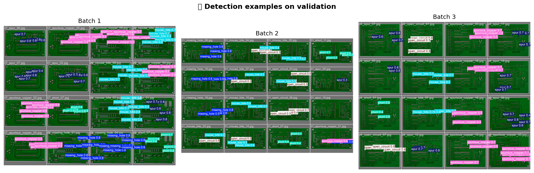
Gallery & Training Visualizations
How to Clone and Run the Project Locally
Copy and paste the commands below into your terminal to clone the repo and run the desktop testing app:
git clone https://github.com/alainpaluku/pcb-defect-detection.git
cd pcb-defect-detection
pip install -r requirements.txt# Placez votre fichier pcb_model.pt dans le dossier models/
# Placez vos images PCB de test dans le dossier images/python -m gui_test.appGPU Training on Kaggle Notebooks
!pip install ultralytics -q
!wget -q https://github.com/alainpaluku/pcb-defect-detection/archive/main.zip
!unzip -q main.zip
!mv pcb-defect-detection-main pcb-defect-detector
%cd pcb-defect-detector
!python run_kaggle.py